Advanced Semiconductor Packaging – The Great U.S. Imperative
Angie Kellen, Director, Client Services, Open Sky Communications
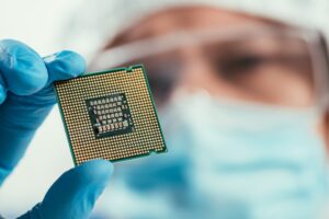
Image Source: Georgia Tech
Semiconductors, or chips, power our consumer electronics, data centers, critical infrastructure, automobiles, and virtually all military systems. They are also key building blocks of the technologies that will shape our future, including artificial intelligence (AI), biotechnology, and clean energy. The United States has remained a global leader in semiconductor design and research and development, but it has fallen behind in manufacturing. The U.S. share of global semiconductor manufacturing capacity plummeted from nearly 40% in 1990 to approximately 12% by 2022. Today, none of the most advanced logic and memory chips are manufactured at commercial scale in the United States. These are the chips driving PCs, smartphones, and supercomputers. In addition, many elements of the semiconductor manufacturing supply chain, in particular, advanced packaging, are geographically concentrated outside of the U.S. This leaves us vulnerable to disruption and endangers the global economy and our national security.
In the rapidly evolving landscape of semiconductor technology, advanced packaging has emerged as a critical frontier. As the demand for high-performance computing (HPC), AI, and 5G technologies accelerates, the United States has finally recognized the strategic imperative to bolster its domestic capabilities in semiconductor advanced packaging. This blog takes a high-level look at the current state of advanced packaging in America, the driving forces behind its development, the key players shaping its trajectory, and the geopolitical dynamics influencing its progress.
Advanced packaging refers to the innovative methods of assembling semiconductor devices, enabling enhanced performance, reduced power consumption, and greater functionality. Unlike traditional packaging, which involves placing a single chip into a package, advanced packaging techniques allow for the integration of multiple chips into a single package, facilitating faster communication between components and improved overall efficiency.
Some of the current advanced packaging technologies include:
Fan-Out Wafer-Level Packaging (FOWLP) where chips are embedded in a mold compound and then rerouted using redistribution layers (RDLs).
3D Packaging / 3D-IC stacks the dies vertically and they are interconnected using through-silicon vias (TSVs).
System-in-Package (SiP) combines multiple heterogeneous components (CPU, memory, RF, sensors, etc.) into a single package.
Chiplet-Based Packaging uses smaller functional blocks called chiplets that are interconnected via high-speed interconnects like UCIe.
Flip-Chip Packaging flips the die and is connected directly to the substrate using bumps or solder balls as opposed to traditional wire bonding.
Package-on-Package (PoP) stacks multiple packages (like logic and memory) on top of each other and they are interconnected.
Advanced packaging is driving the next wave of semiconductor innovation by allowing better performance, higher density, and more efficient integration of different components. It’s becoming a critical enabler for AI, 5G, HPC, and other cutting-edge applications as traditional transistor scaling slows down.
Why is it so necessary for the U.S. to have its own domestic, high-volume advance packaging capabilities?
First, we need to maintain our national security and technological leadership in the world. Semiconductors are at the foundation of our modern defense systems and critical infrastructure. Ensuring that advanced packaging processes occur within the U.S. safeguards sensitive technologies and maintains the integrity of defense applications. Leading in advanced packaging is paramount for the U.S. to retain its position at the forefront of technological innovation, particularly in emerging fields like AI and quantum computing.
Second, we need to establish supply chain resilience. Remember the COVID-19 pandemic? It identified the many vulnerabilities in our supply chains that were a result of relying heavily on overseas semiconductor manufacturing and packaging, along with other goods and services. With a significant portion of advanced packaging capabilities concentrated in Asia, particularly Taiwan and South Korea, the U.S. faces risks associated with geopolitical tensions and logistical challenges. Establishing robust domestic advanced packaging infrastructure is essential to mitigate these risks and to ensure a resilient supply chain.
What are we doing to get there?
The U.S. is leveraging a combination of key government initiatives and investments along with collaborations with public and private companies in the semiconductor industry to enable domestic chip manufacturing. The Creating Helpful Incentives to Produce Semiconductors (CHIPS) and Science Act, enacted to revitalize the U.S. semiconductor industry, allocates substantial funding toward advanced packaging. In January 2025, the U.S. Department of Commerce announced $1.4 billion in awards to support the National Advanced Packaging Manufacturing Program (NAPMP).
The following companies have received funding for advanced packaging innovations:
Image Source: Tecovedas
Absolics, Inc. in Covington, Georgia, $100 million in direct funding. This award will support Absolics’ Substrate and Materials Advanced Research and Technology (SMART) Packaging Program and help build a glass-core packaging ecosystem. Absolics’ glass substrates will be used as an important advanced packaging technology to increase the performance of leading-edge chips for AI, HPC, and data centers by reducing power consumption and system complexity.
Applied Materials, Inc. in Santa Clara, California, $100 million in direct funding. This project will develop and scale a disruptive silicon-core substrate technology for next-generation advanced packaging and 3D heterogeneous integration. Applied Materials’ silicon-core substrate technology has the potential to advance America’s leadership in advanced packaging and help catalyze an ecosystem to develop and build next-generation energy-efficient AI and HPC systems in the U.S.
Arizona State University in Tempe, Arizona, $100 million in direct funding. The award will support the development of the next generation of microelectronics packaging through FOWLP. Centered at ASU’s Advanced Electronics and Photonics Core Facility, this project supports ASU’s research in exploring the commercial viability of 300-mm wafer-level and 600-mm panel-level manufacturing, a technology that does not exist as a commercial capability in the U.S. today.
Natcast’s Advanced Packaging Facility in Tempe, Arizona, $1.1 billion in direct funding. The award will enable Natcast to operate and manage the CHIPS NAPMP advanced packaging capabilities that will be co-located with NSTC prototyping capabilities at the recently announced CHIPS for America NSTC Prototyping and NAPMP Piloting Facility (PPF) in Tempe, Arizona. Key packaging capabilities funded by this award are expected to include a baseline advanced packaging piloting line to enable the development and commercialization of new advanced packaging processes. The CHIPS for America PPF will feature cutting-edge capabilities to bridge the gap between laboratory research and full-scale semiconductor production. This facility will enable researchers and industry leaders to develop and test new materials, devices, and advanced packaging solutions in a state-of-the-art R&D environment.
Several semiconductor industry leaders are actively contributing to the expansion of advanced packaging in the U.S.:
NVIDIA. The leading computer chipmaker has announced plans to invest several hundred billion dollars over the next four years to manufacture semiconductors and electronics in the U.S. This strategic move aims to mitigate risks associated with geopolitical tensions and supply chain vulnerabilities. NVIDIA’s efforts are supported by investments from suppliers like Taiwan Semiconductor Manufacturing Company (TSMC), which has committed $100 billion to its Arizona site, enabling the production of NVIDIA’s top-tier Blackwell chips in the U.S.
Amkor Technology. A prominent provider of semiconductor packaging and test services, Amkor plans to build a state-of-the-art, $2 billion manufacturing facility in Arizona to support TSMC’s nearby semiconductor plant that is under construction. With Apple as one of the largest customers, Amkor expects the facility to be the biggest advanced packaging operation in the U.S. encompassing over 500,000 square feet of clean room space. The facility aims to offer high-volume, leading-edge technologies for advanced packaging and testing of semiconductors, catering to critical markets such as HPC, automotive, and communications.
Intel. As one of the few semiconductor firms operating large-scale advanced packaging facilities in the U.S., Intel plays a pivotal role in domestic packaging capacity. Building on the company’s existing $100 billion investment, the U.S. Department of Commerce has awarded Intel up to $7.86 billion in direct funding through the CHIPS Act to advance Intel’s commercial semiconductor manufacturing and advanced packaging projects in Arizona, New Mexico, Ohio and Oregon.
TSMC. The world’s largest dedicated semiconductor foundry, TSMC announced its intention to expand its investment in advanced semiconductor manufacturing in the U.S. by an additional $100 billion. Building on the company’s ongoing $65 billion investment in its advanced semiconductor manufacturing operations in Phoenix, Arizona, TSMC’s total investment in the U.S. is expected to reach US$165 billion. The expansion includes plans for three new fabrication plants, two advanced packaging facilities and a major R&D team center, solidifying this project as the largest single foreign direct investment in U.S. history.
What are the challenges that can derail this momentum? Image Source: News-Clearance Jobs
The U.S. semiconductor industry is navigating a complex geopolitical landscape that both propels and impedes the advancement of domestic advanced packaging capabilities. The global semiconductor landscape is deeply intertwined with geopolitical considerations.
U.S.-China Trade Relations. The Trump administration’s export restrictions on advanced AI chips to China have impacted companies like NVIDIA and AMD, with NVIDIA anticipating a $5.5 billion financial hit due to limitations on exporting high-performance components. The on-again, off-again tariffs and trade war is causing uncertainty in the semiconductor market.
Taiwan’s Role. Taiwan’s Economy Minister announced plans to run simulations, or studies, on how possible U.S. tariffs (taxes on imports) could impact Taiwan’s semiconductor industry, which plays a central role in its economy. Taiwan is preparing for the possibility that the U.S. might put tariffs on Taiwanese semiconductors, and wants to negotiate with the U.S. to avoid being treated unfairly.
Legislative Support. The CHIPS Act, which passed the US Congress with bipartisan support, has been instrumental in spurring significant investments in domestic semiconductor manufacturing. With the Trump administration considering shutting down the program, repealing such legislation could jeopardize national security by hindering the growth of domestic advanced packaging capabilities.
Global Investments. In addition to previous examples, companies like SK Hynix are investing heavily in U.S. advanced packaging facilities, with a $3.9 billion project in Indiana, reflecting a strategic shift to diversify manufacturing locations. Headquartered in South Korea, SK Hynix is the world’s leading producer of high-bandwidth memory that speeds the performance of AI chips.
The Road Ahead
The semiconductor industry is at a critical stage, with unprecedented growth opportunities driven by AI and other emerging technologies. The advanced semiconductor packaging market is poised for robust, double-digit growth through 2030 as value creation shifts decisively from front-end scaling to back-end integration. The advanced packaging market is projected to grow from nearly $18.1 billion to $29.8 billion by 2031, a CAGR of 7.5% during the forecast period.
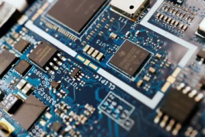
Image Source: World Economic Forum
By leveraging ongoing collaboration, innovation, and strategic policymaking, the U.S. will strengthen and solidify its leadership in the global semiconductor landscape.