Laser Beams (Without the Sharks) at the Core of Modern Chips
Angie Kellen, Director, Client Services, Open Sky Communications
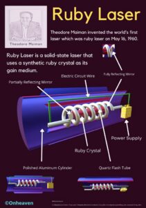
Source: OnHeaven
On May 16, 1960, Theodore Harold Maiman successfully fired the first working laser at Hughes Research Laboratories in Malibu, California, the research arm of the Hughes Aircraft Company. Maiman’s solid-state, pink ruby laser emitted mankind’s first coherent light.
Annually on May 16th, the International Day of Light celebrates that groundbreaking achievement, which marked the beginning of laser technology. And while it may not have looked like science fiction at the time, it quietly set the stage for a very real, laser-powered world. A world that pop culture would soon exaggerate in unforgettable ways.
There’s a segment in the movie Austin Powers: The Spy Who Shagged Me where Dr. Evil demands to have “sharks with frickin’ laser beams attached to their heads.” If you are unfamiliar with this movie, here is a clip of this scene. It’s ridiculous, theatrical, and intentionally disconnected from reality. Long before Austin Powers, science fiction like Buck Rogers comic books introduced audiences to laser pistols, energy weapons, and sleek, futuristic technology all powered by beams of light. Back then, lasers were a type of shorthand that represented “the future.” They were flashy, powerful, and a little mysterious. After more than two decades in the semiconductor industry, I can say that lasers have, in their own way, lived up to the hype, but not in the way Hollywood imagined.
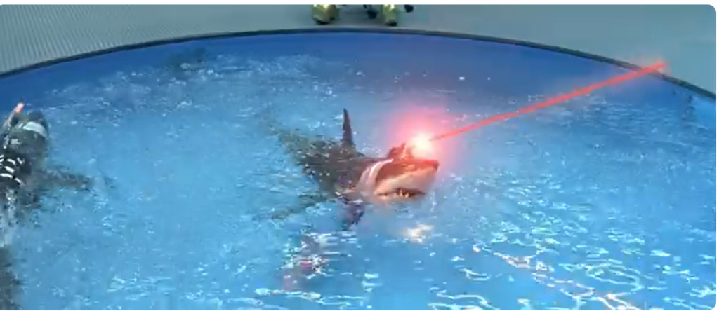
Shark with ‘frickin’ laser beam attached to its head. Source: Austin Powers: The Spy Who Shagged Me (1999), © New Line Cinema. Image used for editorial/commentary purposes under fair use.
What’s fascinating is that while we aren’t quite at the point of laser pistols battling down spaceship hallways, we did end up with something even more impactful. Lasers have been quietly inserted into the infrastructure of modern life, enabling the devices, networks, and systems we rely on every day. In my previous blog, “Photonics—The World’s Invisible Engine,” I covered how photonics has crept out from the research labs to quietly become a foundational part of how we live and work. Lasers are another technology that has similarly been around for some time but has quietly become a critical enabler for modern chips and in turn, our digital world.
The glare from the constant hype of artificial intelligence (AI) and its ever-growing applications and uses have cast a shadow on other advances, like laser technologies. We all enjoy the benefits of lasers every day and don’t even realize it. While there are many military applications above my security clearance and equally as many uses of LiDAR technology in the world, this blog will explore some of the ways in which laser technologies are impacting today’s chips and digital devices. And if you’ve spent as much time as I have in the semiconductor industry, you start to realize that the real story of lasers is less about spectacle and more about precision, control, and evolution.

Source: Buck Rogers comic art, © respective rights holders. Used for editorial purposes.
When I first entered the semiconductor world, lasers were already part of the semiconductor manufacturing ecosystem, but they weren’t front and center. The attention was on scaling, yield, and lithography systems as a whole and not necessarily the laser technology behind them. My first client was a lithography equipment provider. At the time, lasers felt more like specialized tools than part of the manufacturing infrastructure. You knew they were critical, but they weren’t the headline.
Compare that to today, where lasers are not only essential to manufacturing but are increasingly becoming part of the end-product itself. That shift didn’t happen overnight. It came through incremental innovation, driven by the relentless pursuit of smaller nodes, higher performance, and tighter tolerances. If Buck Rogers imagined lasers as the defining technology of the future, he wasn’t entirely wrong, he just didn’t foresee that their most important role would be inside cleanrooms over their use on battlefields.
Photolithography remains the backbone of semiconductor manufacturing, and lasers are at its core. Modern systems, especially extreme ultraviolet (EUV), rely on high-energy laser pulses to generate plasma that emits extremely short wavelengths of light. These wavelengths allow us to pattern features on a wafer at the nanometer scale. ASML has cornered the market on providing EUV lithography systems that enable high-volume manufacturing at the nanoscale. If you are interested, ASML provides a great explanation of lithography, light and lasers.
What’s remarkable is not just the science, but the consistency. These laser systems fire with extraordinary precision, millions of times over, maintaining stability at scales that would have seemed impossible when I started in the industry. This is where the science fiction comparison starts to feel almost understated. In Buck Rogers, lasers were dramatic and visible. In a modern fab, they’re invisible, controlled, and arguably far more powerful in their impact.
Laser Annealing
Thermal processing is another area where lasers have fundamentally changed the game. In earlier days, furnace annealing was the standard. You basically baked the wafer to a specified temperature to get the desired reactions. It worked, but it was cumbersome. You were heating entire wafers when you often only needed to affect a very specific region. Laser annealing, sometimes called laser spike annealing, changed that dynamic completely. Now, energy can be delivered with extreme localization and timing, down to nanoseconds, activating dopants and repairing crystal structures without disturbing surrounding material.
Back to my first client. In addition to lithography, they had developed very advanced systems providing laser annealing. The process was way ahead of its time and designed for very advanced nodes, which the industry was currently unable to achieve. The laser that was used in these systems was the most advanced for its day. When a client ordered a laser annealing tool, mainly for R&D, they would have to carve out a good section of space below the fab floor to accommodate the weapons-grade laser that was needed for the process. Today, with the continued innovations in lasers, there is no need to dig into the fab’s subfloor just to house the laser. My client licensed its laser thermal annealing technology to another company, and now it is right on time for today’s nodes.
Applied Materials, a giant in the semiconductor space, provides a good explanation of its laser annealing system and why it is important. From my perspective, this is one of the clearest examples of how lasers brought surgical precision into semiconductor manufacturing. It’s less “laser cannon” and more “laser scalpel,” and this distinction matters.
Dicing and Advanced Packaging
As the industry has shifted toward advanced packaging and heterogeneous integration, including chiplets and 3D stacking, lasers have taken on a more visible and mechanical role. Laser dicing allows wafers to be cut with minimal stress, cleaner edges, and higher yields. That becomes critical as designs grow more complex and margins for error shrink. 3D-Micromac provides laser micromachining services and they have a nice video that illustrates laser-based wafer dicing. This is one of those areas where the physicality of lasers becomes more tangible. You can almost draw a line from the imagined “laser cutting tools” of science fiction to the very real systems slicing through wafers today. Except instead of sparks and drama, it’s all happening in a highly controlled, particle-free environment.
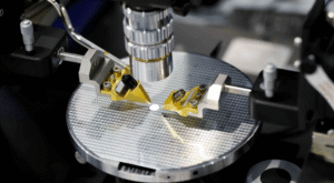
Laser-based defect inspection on a semiconductor wafer. Source: Inquivix Technologies
Inspection and Metrology
Another critical application is inspection and metrology. As features shrink, the margin for error becomes microscopic. Laser-based systems provide the resolution needed to detect defects, measure dimensions, and ensure consistency across wafers. With the move to smaller and smaller geometries, lasers provide the ability to detect the undetectable. Averroes is a company that combines AI technology and lasers to enable faster and more accurate results. They provide a good explanation of the difference between laser-based metrology and inspection. These types of systems don’t get much attention outside the industry, but they’re essential. Without them, yield drops, costs rise, and innovation slows. In a way, they’re the humble unsung heroes, not very flashy, but like an incredibly precise set of eyes that never blink. This is a perfect example of innovation that continues to advance critical capabilities that enable today’s chips to get smaller with higher performance, all unseen by the consumer.
Wafer Bonding
Lasers aren’t just transforming how we inspect wafers; they’re now reshaping how we assemble them, enabling the next leap in 3D semiconductor scaling. As the industry pushes beyond the limits of traditional 2D scaling, lasers have become essential tools for new manufacturing approaches. Their precision, low‑thermal‑impact energy delivery, and ability to interact cleanly with advanced materials make them ideal for processes that demand atomic‑level control. This is especially critical as the roadmap shifts toward 3D integration, where stacking wafers and extremely thin material layers is necessary. 3D integration enables emerging architectures such as new memory technologies, backside power delivery networks, and even future transistor concepts like complementary field-effect transistors (CFETs).
Wafer bonding is at the center of this transformation. By joining multiple wafers or material layers with extremely high alignment accuracy, bonding unlocks the vertical dimension of semiconductor scaling. EV Group (EVG) has been a leader in advancing this capability, and its new IR LayerRelease™ technology represents a major breakthrough. IR LayerRelease uses an infrared laser that passes through silicon, which is transparent to the IR laser wavelength, to initiate clean, controlled debonding. When combined with specially formulated inorganic release layers and silicon carrier wafers, this approach enables nanometer‑precision separation of ultra‑thin film layers without the need for glass substrates, which are not compatible with the high temperatures required for semiconductor front-end processing. By enabling the use of silicon wafer carriers, IR LayerRelease overcomes the temperature limitations of glass carriers and opens up entirely new process flows for 3D IC and 3D sequential integration applications. My experience with EVG has taught me that laser‑enabled wafer bonding isn’t just a manufacturing technique, it’s an essential capability for the semiconductor roadmap ahead.
Embedded Lasers and Silicon Photonics
I saved the most amazing for last. If there’s one area that truly feels like science fiction made real, it’s silicon photonics. As I noted in my previous blog on photonics, lasers are no longer just external tools. They’re integrated into chips, enabling data transmission through light rather than electrical signals. What makes this shift so significant is the breaking of a long-standing bottleneck. For decades, we’ve relied on electrical interconnects to move data within and between chips. But as bandwidth demands skyrocket, driven by AI, cloud computing, and hyperscale data centers, those electrical pathways are hitting physical limits in terms of speed, power consumption, and heat. Silicon photonics changes that equation entirely. By moving data with photons instead of electrons, we unlock dramatically higher bandwidth, lower latency, and improved energy efficiency.
From an industry perspective, this is more than just an incremental improvement, it’s an architectural shift. We’re now seeing co-packaged optics, optical I/O, and integrated laser sources becoming part of real product roadmaps, not just research projects. The idea of placing lasers directly on or near the chip to enable high-speed optical links is quickly moving from “bleeding edge” to “expected capability,” especially in environments where moving massive amounts of data quickly is essential.
This is also where manufacturing complexity ramps up in a very real way. Integrating lasers into silicon isn’t trivial. It involves material challenges, thermal management considerations, and alignment precision that pushes the limits of current manufacturing techniques. In many cases, it requires hybrid approaches to efficiently generate light. Watching how the industry has navigated these challenges over the years has been nothing short of impressive, and it’s a testament to how far both laser technology and semiconductor integration have come. If you want more information, Intel’s work in this space is a great reference point, particularly as they continue to push silicon photonics into data center and high-performance computing applications.
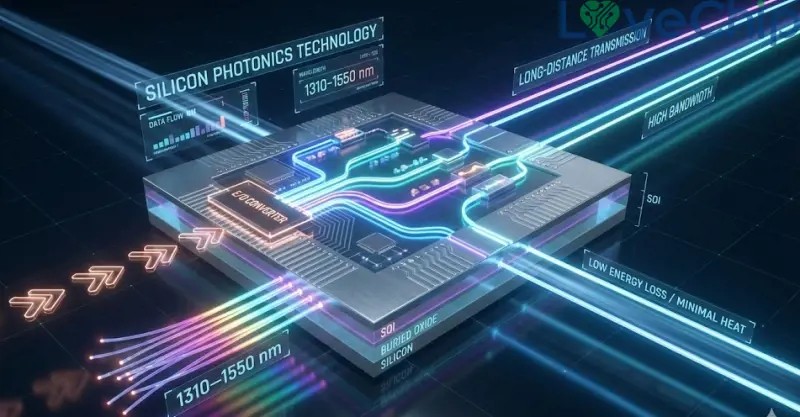
Silicon Photonics Diagram. Source: Love Chip
This is the moment when the Austin Powers joke starts to feel surprisingly relevant. We may not have “laser beams attached to sharks” yet, or at least not known to the public, but we do have laser sources embedded in silicon, driving communication at speeds and efficiencies that traditional electronics struggle to match.
And unlike science fiction, where lasers are often about destruction or visibility, these are about connectivity, efficiency, and scale. They’re invisible and powering the capabilities to create AI training clusters to global data networks, quietly doing exactly what science fiction promised, just without the dramatic soundtrack.
Looking forward, the role of lasers will only expand. They’re becoming more efficient, more compact, and more deeply integrated into both manufacturing processes and end products. As AI, high-performance computing, and data infrastructure continue to grow, the demand for optical solutions will only rise. Integrated photonics, optical interconnects, and advanced packaging will all rely heavily on laser technologies. After 20+ years in this field, one thing is clear: lasers have transitioned from specialized tools to critical process infrastructure in semiconductor manufacturing. They’re no longer optional. They’re essential.

TV Remote. Source: Envato
Science Fiction Got the Spirit Right
Science fiction didn’t get everything right. We don’t have intergalactic laser battles or underwater sharks equipped with laser-beam weapons, again not as far as the public has been informed. But it did get one thing right: lasers matter. From Buck Rogers to Austin Powers, lasers have always symbolized the future. What’s changed is how that future actually showed up.
It turns out the real revolution wasn’t flashy. It was precise, methodical, and deeply embedded in processes most people will never see. And maybe that’s the most interesting part of all. Because while Dr. Evil was asking for “frickin’ laser beams,” the semiconductor industry was quietly building a world where lasers are everywhere, just hidden in plain sight.